
3. 先端実装関連の動き
引き続く激動の中、エレクトロニクス・半導体業界は、新しい要素技術、プロセス技術を駆使した新しい分野の開拓、展開が依然旺盛に行われて、市場需要を大きく支えている。
伸びが減速したとはいえ、大規模な世界市場を維持するスマートフォンに加えて、Internet of Things(IoT)、データセンター、自動運転車、スマートエレクトロニクスなどの新しい分野が、人工知能(artificial intelligence:AI)、深層学習(deep learning)はじめ要素技術の目覚ましい深化、高度化から市場のより大きな一角を担うようになっている。
このような状況の中、先端実装関係でも引き続き、
○ 新分野の高性能化、高機能化に向けた貫通電極(TSV:Through Silicon Via)、シリコンインターポーザ、chipletなどを駆使したSystem in Package(SiP)化のアプローチ
○ 3D NANDに代表されるメモリ半導体での多層化による大容量化の継続進展が前面に出て、それぞれ大きく引っ張る技術そして業界模様が続いている。
Moore則後の進化、展開の実現手段の大きな1つとして先端実装へ注目度が一層高まってきているこの1年の動きを次のように項目分けしてまとめている。
・ 技術および市場評論
・ 国際会議および展示会
・ 3D NANDはじめメモリ関係
・ 各社・機関の取り組み
・ 政府・業界関連の動き
・ 研究関連
2020年10月から2021年9月までの動きについて、以下、それぞれ基本時間順に示していく。
1.技術および市場評論
先端実装市場の規模の見方があらわされている。
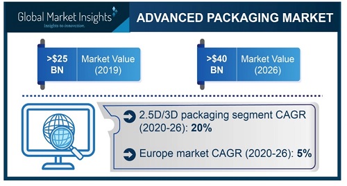
◎Advanced Packaging Market to Witness Steady Growth of 8% During 2020-2026 (10月8日付け SEMICONDUCTOR DIGEST)
→Global Market Insightsの最新調査。先端実装市場が、現在の$25 billionを上回る規模から2026年までに$40 billion超に延び、著しい牽引力を得ていく。
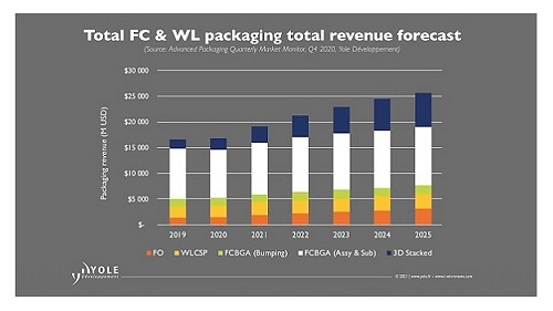
◎Advanced packaging to have 31% CAGR 2019-25
-Yole: Advanced packaging on pace to reach $4B by 2025(11月5日付け Electronics Weekly(UK))
→Yole Développement発。high-end実装市場が、2019年と2025年の間で31%のCAGR、2025年までに$4 billionを上回る規模に達する。
◎Emerging Apps And Challenges For Packaging
-Heterogeneous integration advances, slowly yet surely
(11月23日付け Semiconductor Engineering
→車載electronics, サーバおよびスマートフォンにおけるheterogeneous integrationに向けた先端IC実装の開発が受け入れられてきているが、complexityおよびコストが依然課題。Yole Developpementは、昨年の先端実装市場が$29 billionの規模と評価、年に6.6%増大して5年で$42 billionになると予測。
◎North America Advanced Packaging Market 2026
- A $5 Billion Revenue Opportunity(1月20日付け SEMICONDUCTOR DIGEST)
→Graphical Research発。
北米先端実装市場売上げが2019年に$3 billionを越え、2026年までに5 billion-dollar台に達する見込み、2020年から2026年の間に7%/年で伸びていく。
◎ Advanced packaging market growing 6.6% CAGR to reach $42bn in 2025
-Yole: Advanced packaging market to hit $42B in 2025 (3月1日付け Electronics Weekly(UK))
→Yole Developpementの予測。先端実装市場が、2019-2025年の間6.6%のCAGRで伸びて、2025年には$42 billionに達すると見る。
◎3D Semiconductor Packaging Market Growth Opportunities in the Forthcoming Years with Forecast to 2023 (6月16日付け SEMICONDUCTOR DIGEST)
→Market Research Future(MRFR)の最新レポート。
グローバル3D半導体実装市場が、2023年末までに$37,472.7 millionの規模に達する様相、健全な成長率を反映の旨。
3D半導体実装は革新的な技術であり、いくつかの利点がある。
半導体をコア単位で製造して後からレゴブロックのように合体させることで1つの製品をつくり出す方式、chipletが、やはり最も注目のキーワードであり、さまざまな切り口の評論が見られている。
◎Protecting Chiplet Architectures With Hardware Security
-Chip disaggregation means a larger attack surface, increasing the chances of a successful trojan or man-in-the-middle attack.(10月8日付け Semiconductor Engineering)
→Rambus Securityのtechnical director、Scott Best氏記事。
chipletsは、半導体性能、コストおよびtime to marketを進める上で動かずにはいられない利益を与えることで、大きな牽引力を得ている。
Moore's Lawが鈍化、より強力な半導体の構築はより大きな半導体の構築になっていく。
しかし半導体寸法がreticle限界を押しやって、半導体の大きさの伸びはますます実用的でない。
chipletsは、大きいmonolithic integrated circuits(ICs)をより小さなpiecesに分解して新しい道筋が得られ、system-in-package(SiP)で一緒に利用できる。
◎Explainer on Packaging: Interposers, Bridges and Chiplets
(11月10日付け EE Times)
→IC業界が先端実装への重点化を更新しており、chipletsは最も熟さない選択肢であるが、最も広く行き渡る1つでもある。
◎Designs Beyond The Reticle Limit
-Big, complex chip designs exceed reticle limits
-Chips are hitting technical and economic obstacles, but that is barely slowing the rate of advancement in design size and complexity.(11月12日付け Semiconductor Engineering)
→IC設計の複雑度および寸法が増大、technologistsが先端photolithographyで用いられるreticlesによる物理的制約を越える問題を扱っている旨。
「代表的には、設計が粗いレベルで2.5D chiplet境界にわたって分割されると見ている。」と、Armのvice president of technology and fellow、Peter Greenhalgh氏。
◎Apple M1 Processor, Passing on the Chiplets (11月13日付け EE Times)
→今週のAppleのM1プロセッサ発表に照らして、Appleがなぜchipletsを通り過ぎたか、chipletsはどこで理に適うか、考えたい。
◎Chiplets For The Masses
-Analysis: Chiplet tech moves from the few to the many
-Chiplets are technically and commercially viable, but not yet accessible to the majority of the market.
How does the ecosystem get established? (3月3日付け Semiconductor Engineering)
→chiplet技術は、選ばれた数少ない半導体会社に限られて、chipletsの採用 が広まるには強力なecosystemおよび業界標準が必要となる旨。
「健全な技術的考え方であり、動きを起こそうとしている団体がある。」と、Ansysのdirector of product marketing、Marc Swinnen氏。
◎Chiplets: A Short History (3月14日付け EE Times)
→用語がいつ普及するようになったか、考えるのに、Google Trendsは2004年に遡る検索用語としてchipletの歴史を与えている。
chipletで初期のちょっとの手出しがあったが、すばやく消えて、本当に上がってきたのは2019年以降。
◎More than Chiplets | Facebook Enters the Fray (3月16日付け EE Times)
→Facebookによるデータセンター向けハードウェアの仕様や設計図を公開するプロジェクト「Open Compute Project(OCP)」。
Chipletsが、OCPのsubgroup, Open Domain Specific Architecture(ODSA)に属し、programmableデバイスも研究されている。
◎Waiting For Chiplet Standards
-Chiplet standards are starting to emerge
-An ecosystem is required to make chiplets a viable strategy for long-term success, and ecosystems are built around standards. Those standards are beginning to emerge today. (3月25日付け Semiconductor Engineering)
→chiplet技術が、業界標準が開発されていてより多くのユーザにchipletsを利用できるようにするところまで成熟してきている旨。
「このことはこの領域で各社が見るたくさんの課題を緩和していく本当のopportunityである。」と、CHIPS Allianceのexecutive director、Rob Mains氏。
◎CEO Outlook: Chiplets, Longer IC Lifetimes, More End Markets
-Experts discuss chiplet tech, other topics
-How the end of scaling and the electrification of everything are changing chip design.
(7月14日付け Semiconductor Engineering)
→半導体業界のトップexecutivesの7人がchiplet使用、末端市場およびIC長寿命化を議論するroundtable interview。
「我々のたくさんのパートナーが、複雑性増大への対応、およびかつてない高効率のシステムを構築する方法としてchipletsに非常に興味を持っている。」と、ArmのCEO、Simon Segars氏。
◎Piecing Together Chiplets
-Overcoming the challenges of chiplets
-Changes that could push this packaging approach into the mainstream, and the challenges ahead. (7月22日付け Semiconductor Engineering)
→chiplet技術の使用が、半導体業界においてより普通になってきている旨。「来年はchiplet設計の数が増えていく。」と、TechSearch Internationalのpresident、Jan Vardaman氏。
◎EXPLAINER-Intel banks on 3D chip technology to win over new customers (7月26日付け Reuters)
→半導体製造における最新の競争として、単一の大きな半導体をつくろうとするのではなく、取り出した微小なsquares、“chiplets”あるいは“tiles”の重ね合わせである。
◎Challenges With Chiplets And Packaging
-Experts discuss advanced packaging, chiplets, and more
-Experts at the Table: The impact of optics, copper hybrid bonding, more standardized interconnects, and many other technologies under development. (9月15日付け Semiconductor Engineering)
→先端IC実装, chiplets使用, interconnects, copper hybrid bondingおよびopticsなどいろいろな話題を5人の業界エキスパートが話し合うroundtable interview。
「chipletsに進むと、最初の応用がhigh-endシステムになっていくのは明らか。」とPromexのPresident and CEO、Richard Otte氏。
「すべてcustomになっていく。」
先端実装の現状および課題についての見方が、いろいろあらわされている。
◎Defect Challenges Grow For IC Packaging
-Defects emerge in advanced chip packaging
-New equipment will help, but it's expensive and requires more steps. (10月22日付け Semiconductor Engineering)
→先端IC実装が新たないろいろな欠陥に悩まされており、次世代検査装置の開発を必要とする。
◎Designing 2.5D Systems
-2.5D IC designs create new challenges
-Connecting dies using an interposer requires new and modified processes, as well as organizational changes.(3月15日付け Semiconductor Engineering)
→2.5D半導体設計におけるシリコンインタポーザ使用など先端実装技術の採用増大から、新しいビジネス、組織的および技術的課題一式があらわれている。
「2D設計とまったく同様、初期floorplanningを行わなければならないし、architectは何が下流でやってくるか気づく必要がある。」と、Cadence Design Systemsのsenior director, product management、Vinay Patwardhan氏。
◎What Goes Wrong In Advanced Packages
-The challenges of advanced IC packaging
-More heterogeneous designs and packaging options add challenges across the supply chain, from design to manufacturing and into the field.(3月24日付け Semiconductor Engineering)
→microchipsに向けた先端実装の種類の広がりで、複雑性増大、lifetimesの変化および独特の設計によりいくつかの問題が示される旨。
「標準が、high volume達成に向け、そして不具合へのインパクトを高めるのに必要となる。」と特に言及するSynopsysのpackage design engineer、Kent Stahn氏。
◎3D Stacking For Performance And Efficiency
-Testing the feasibility and readiness of high-density, face-to-face, wafer-bonded 3D stacking technologies.(4月8日付け Semiconductor Engineering)
→Moore's Law scalingが鈍化、あるプロセスnodeから次への性能、power, area, およびコストの改善が抑えられる旨。
結果として、先端実装および3D stacking技術が次世代高性能高エネルギー効率設計に向けたkey driversとして最前線に出てきている。
◎DRAM Destined to be 3D
-3D DRAM will be different than 3D NAND from a materials perspective(5月11日付け EE Times)
→数年かかるかもしれないが、DRAMがNANDの歩みに従って3Dに向かう様相、コスト効率良く行うには新しい製造装置および材料が必要になる旨。
◎Advanced Packaging's Next Wave
-The next wave in advanced packaging technology
-A long list of options is propelling multi-chip packages to the forefront of design, while creating a dizzying number of options and tradeoffs(5月20日付け Semiconductor Engineering)
→先端実装技術が、IC組立&テスト会社で使われてきている旨。
「microbumpsがstackingに向けて使えるには、個々の高さおよびdie-level coplanarityが非常に正確、高精度に測られなければならない。」と、Onto Innovationのdirector of thin films product management、Priya Mukundhan氏が論文にて。
◎Bumps Vs. Hybrid Bonding For Advanced Packaging
-Advanced packaging tech: Hybrid bonding or bumps?
-New interconnects offer speed improvements, but tradeoffs include higher cost, complexity, and new manufacturing challenges.
(6月23日付け Semiconductor Engineering)
→先端IC実装技術の実行において、半導体メーカーはinterconnectに向けて従来のcopper microbumpsとcopper hybrid bondingの間の選択となる。
「重要課題の1つとして、特にbondingプロセスの間に低温化bondingおよびalignment精度改善を要する応用について、コスト効率の良い統合方式の発案がある。」と、Lam Researchのmanaging director of the advanced packaging business segment、Manish Ranjan氏。
◎Advanced Packaging Technologies Overcoming the Memory System Performance and Capacity Limitation (7月21日付け EE Times)
→SK hynixのHo-Young Son, Ph.D.氏による先端実装技術に焦点を当てた記事。
以下の項目:
Rethinking packaging technology
Memory Capacity Demands Impact Chip Technology
Balancing Capacity and Heat Generation
Transforming Packaging for Growth
◎WF6 and NF3 Demand Expected To Outstrip Supply By 2025 Driven By 3D NAND Memory Evolution
(8月10日付け SEMICONDUCTOR DIGEST)
→TECHCET発。
3D NANDメモリの進化で、WF6(tungsten deposition)、NF3(chamber clean gases)、および重希ガス(KrおよびXe)の使用増加が引っ張られ、供給不足につながる可能性がある。
◎Current And Future Packaging Trends
-Experts discuss trends in advanced packaging
-Experts at the Table: Rising costs and the physical limits of reticles is forcing more companies to examine alternatives to shrinking geometries. (8月19日付け Semiconductor Engineering)
→業界エキスパート5人がIC実装の最新の開発について語るroundtable interview。
「bigプレイヤーが、実装の役割を実現している。」と、EV Groupのdirector of business development、Thomas Uhrmann氏。
次章「国際会議および展示会」以下は、「その②」でご紹介する。
- 会社名
- Gichoビジネスコミュニケーションズ株式会社
- 所在地


-
真空リフロー、N2リフロー、エアリフローのことなら、エイテックテクトロン(株)にお任せください。フラックスレス真空リフロー装置販売開始!エイテックテクトロン株式会社
-
アレムコの導電性/熱伝導性接着剤,コーティング材,グリースのことなら(株)エス・エス・アイ株式会社エス・エスアイ
-
独自の加工技術とノウハウで様々な材料にチャレンジ 〜色々なアイデアを生み出して研究者をサポート〜 ムソー工業株式会社 代表取締役 尾針 徹治 氏Gichoビジネスコミュニケーションズ株式会社
-
SEMICON Japan 2023 2023年12月13日(水)〜15日(金)の3日間、東京ビッグサイトにおいて、半導体を中心としたマイクロエレクトロニクスの製造を支える装置/材料産業の総合イベントであるSEMICON Japan 2023が開催された。Gichoビジネスコミュニケーションズ株式会社